|

During the late 1970s NCR had a chip fab located near Dayton, Ohio, the original home of the Wright brothers. NCR engineers drew a miniature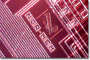 replica of the airplane that the brothers flew in Kitty Hawk, North Carolina and placed this rendition on one of their RAM chips. See if you can pick it out as we zoom the magnification on this RAM chip. replica of the airplane that the brothers flew in Kitty Hawk, North Carolina and placed this rendition on one of their RAM chips. See if you can pick it out as we zoom the magnification on this RAM chip.
The digital images presented above were captured using the oblique illuminator built into the microscope head with the assistance of a Dolan-Jenner Model 180 fiber optics illuminator using a 150 watt projection lamp. The light pipes of the illuminator were placed at approximately a 45-degree angle with respect to the optical axis of the microscope and were positioned to evenly illuminate the specimen. In many cases, colored gels were placed into filter holders and attached to the front of the light pipes to add color to the chip surfaces. A 2-inch square section of black paper was placed over the diffusion filter on the stage of the microscope to avoid any glare from transmitted illumination.
This beautiful miniature rendition of the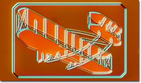 original Wright brothers biplane was discovered on a early 1980s era NCR Microelectronics memory integrated circuit, loaned to us by Greg O'Hara of Marietta, Georgia. This was the first "airplane" to actually fly on its own power with a human pilot. The wingspan of this silicon biplane is 200 micrometers, about 1/60,000 the size of the original (40 feet) plane that was powered by a four-cylinder, 12-horsepower gasoline engine. Orville and Wilbur built the plane in their bicycle shop in Dayton, Ohio (also home of the NCR fab that produced the chip) and shipped it to Kitty Hawk, North Carolina for testing. On December 17, 1903, Orville Wright made the first flight, which lasted 12 seconds and covered 120 feet. Things haven't been the same since. original Wright brothers biplane was discovered on a early 1980s era NCR Microelectronics memory integrated circuit, loaned to us by Greg O'Hara of Marietta, Georgia. This was the first "airplane" to actually fly on its own power with a human pilot. The wingspan of this silicon biplane is 200 micrometers, about 1/60,000 the size of the original (40 feet) plane that was powered by a four-cylinder, 12-horsepower gasoline engine. Orville and Wilbur built the plane in their bicycle shop in Dayton, Ohio (also home of the NCR fab that produced the chip) and shipped it to Kitty Hawk, North Carolina for testing. On December 17, 1903, Orville Wright made the first flight, which lasted 12 seconds and covered 120 feet. Things haven't been the same since.
This flying goose, along with the initials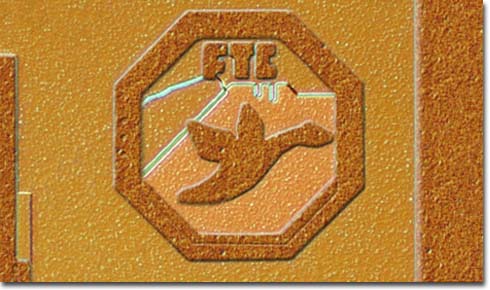 FTC, appears on a number of chips made by NCR Microelectronics (formerly National Cash Register) that were common components on motherboards and peripherals in the 1980s. Gene Fusco of LSI Logic has informed us that these initials represent the location of the NCR design and fabrication facility, located in Fort Collins, Colorado (FTC), that designed and built these chips. The entire image is a derivative work of the logo used by the city, which features several geese flying above Horsetooth Rock, a prominent local landmark in the foothills neighboring Fort Collins. This city is also located along the Rocky Mountain Flyway, a path used by migratory birds including the Canada goose, the bird represented in the logo. FTC, appears on a number of chips made by NCR Microelectronics (formerly National Cash Register) that were common components on motherboards and peripherals in the 1980s. Gene Fusco of LSI Logic has informed us that these initials represent the location of the NCR design and fabrication facility, located in Fort Collins, Colorado (FTC), that designed and built these chips. The entire image is a derivative work of the logo used by the city, which features several geese flying above Horsetooth Rock, a prominent local landmark in the foothills neighboring Fort Collins. This city is also located along the Rocky Mountain Flyway, a path used by migratory birds including the Canada goose, the bird represented in the logo.
We encountered this silicon rendition of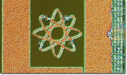 a Bohr atomic model while scanning the surface of an NCR integrated circuit of unknown function. The artwork measures about 40 microns in size and appears to have three individual orbits (atomic orbitals?) with four electrons visible in the orbits. Checking the periodic table of the elements, we discovered that beryllium has an atomic number of four, but this doodle may not be intended to represent the element beryllium. In any event, at 40 microns, the silicon atom on this chip is about 1,300,000 times the size of a single beryllium atom. a Bohr atomic model while scanning the surface of an NCR integrated circuit of unknown function. The artwork measures about 40 microns in size and appears to have three individual orbits (atomic orbitals?) with four electrons visible in the orbits. Checking the periodic table of the elements, we discovered that beryllium has an atomic number of four, but this doodle may not be intended to represent the element beryllium. In any event, at 40 microns, the silicon atom on this chip is about 1,300,000 times the size of a single beryllium atom.
These "mountains" or are a common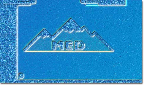 feature on integrated circuits manufactured by the NCR Micro Electronics Division (MED). Former NCR engineer Scott Reedstrom informs us that the mountains are intended to represent Pikes Peak, which is close to the Colorado Springs NCR facility. Scott also mentioned that NCR chip logos were banned around 1985 due to a short caused by the Fort Collins Goose logo, forcing a chip turn. feature on integrated circuits manufactured by the NCR Micro Electronics Division (MED). Former NCR engineer Scott Reedstrom informs us that the mountains are intended to represent Pikes Peak, which is close to the Colorado Springs NCR facility. Scott also mentioned that NCR chip logos were banned around 1985 due to a short caused by the Fort Collins Goose logo, forcing a chip turn.
Source: Molecular Expressions
|

